Research Facilities
Research Equipment
- Nano Fabrication Center
- Materials Characterization Lab
- Environmental Analysis Center
- Synchrotron Radiation Research Center
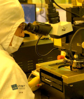
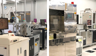
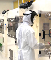
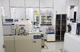
UNIST Nano Fabrication Center
- Clean room: Special closed space for manufacturing semiconductor/sensor device (maintenance of temperature and humidity, control of cleanliness)
- It possesses Class 100 & 1,000 (Class N refers to the number of particles of dust not exceeding N per square foot


Status of Facilities
| Contents | Details | ||
|---|---|---|---|
| Area / Class | 1,000㎡ / 100 | 992㎡ vertical layers with multi-layer structure Yellow zone 100 class and White zone 1,000 class |
|
| Composition of Equipment(units) | Photo | 9 | E-Beam lithography 1, Mask aligner 2, Nano imprint 1, Spin coater 3, 2 microscopes |
| Thinfilm | 14 | Furnace 2, ALD 2, Evaporator 2, LP CVD 1, PE CVD 2, Sputter 2 & etc | |
| Etch | 11 | Deep RIE 1, RIE 2, ICP 2, Asher 1, Wet Station 5 | |
| Inspection & etc | 10 | SEM, Ellipsometer, Profiler, Dicing saw, Bonder, etc | |
| Total | 44 | Capable of one-stop fabrication of multi-layer devices, etc. | |
| Number of processes / rate of operation | 15,000 cases / 46% | It supported more than 15,000 cases of process a year on the basic of unit process with the rate of operation of 46% for the clean room | |
| Area / Class | Establishment of new fabrication | Opening of new fabrication in jan. 2017 after two-fold expansion of its capacity, structure of vertical layers | |
Lithography process
Total process of forming MEMS/NEMS patterns and lift-off
Thin film deposition and etching process
Formation of the structure for deposition and dry etching of insulating nonmetallic thin film (oxide film, nitride film, dielectric thin film, etc.)
Measurement of characteristics of device
Experiment for measurement and analysis of contact / non-contact / electric characteristics / images by self-fabricated specimens
Wet cleaning process
Cleaning and wet etching of the surface of specimens using chemicals
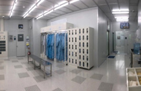 Smock Room
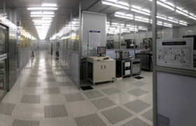 Hallway
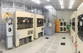 Wet Station
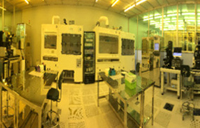 Yellow room
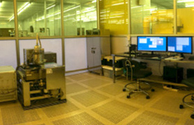 E-beam litho. room
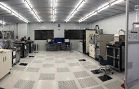 White room#1
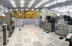 White room#2
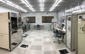 White room#3
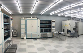 Diffusion room
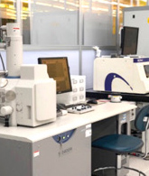
UNIST Materials Characterization Lab
- Equipped with the infrastucture for converged researches in which most advanced and expensive equipment are stacked, the center leads high-precision and high-resolution analysis techniques and supports development of new analysis techniques.


Materials Characterization Lab
| Contents | Details | ||
|---|---|---|---|
| Area (㎡) | 2,061 | ||
| Composition of Equipment (units) | Electron Microscopic Analysis Center | 31 | Advanced TEM, HR-TEM, CS-STEM, Normal-TEM, Bio-TEM, FE-TEM, FIB(3), SEM(5), Ultramicrotome(2), PECS, Electron microscope, equipment for pre-processing of specimens(14) |
| X-ray Analysis Center | 6 | HPXRD, NXRDX, HRXRD, HRPXRD, MPHPXRD, XRF | |
| Thermal and Property Analysis Center | 7 | TGA, DMA, DSC, SDT, Seebeck Coefficient analyser, Dilatometry | |
| Spectrometer Center | 9 | FT-NMR(2), Zeta Potential, FT-IR UV-Vis-NIR Microspectrometer, UV-Vis-NIR(2), AFM-Raman, Confocal Raman | |
| Mass Spectrometer Center | 8 | MALDI-TOF/TOF, GC/MS/MS, LC/MS/MS (ESI-MS), GPC-MALS, DART-HRMS, UPLC/MS/MS, EA(2) | |
| Surface Analysis Center | 7 | TOF-SIMS, XPS, XPS (UPS), AFM (2), BET (2) | |
| Number of analysis / rate of operation | Total number of analyses: 41,501 cases (Internal: 37,987 + Outside companies: 3,421 + Outside individuals: 93) / Average rate of operation of research equipment: 95.7% (As of 2020) | ||
Surface analysis
TOF–SIMS, XPS, XPS/UPS, AFM
Analysis of composition, molecular structure and trace elements of surface 3D analysis through analysis of depth and distribution
Analysis with microscope
TEM(5), SEM(4), FIB(2), Sample prep.
Observation of nano-scale micro structure and electronic imaging with high sensitivity at the atomic level Analysis of diffraction patterns Fabrication of nano device Observation of nano-scale patterning and image
Mass spectrometry
MALDI-TOF/TOF, GC/MS/MS, LC/MS/MS, DART-MS, GPC-MALS, EA(2)
Verification of the molecular weight of macro-oragnic molecules, Analysis of impurities and byproducts, Qualitative / quantitative analysis compounds
Spectral analysis
NMR(2), FT-IR, Raman(2), UV-Vis-NIR(2), UV-Vis Microspectrometer, Fluorometer(3), Zeta sizer
Training of talents having creative knowledge and entrepreneurship Converged education for new materials / chemistry / physics / machinery / infrastructure, etc.joint research project by general / industrial-academic students
X-ray analysis
XRD(6), XRF
Analysis of crystal structure, chemical composition, and physical characteristics of materials or thin films, Analysis of thickness, roughness and density of ultra-thin films and analysis of orientation of substrates and thin films
Thermal and property analysis
Rheometer, thermoanalyzer (4), apparatus for measuring coefficient of thermal expansion, apparatus for measuring thermoelectric modules
Measurement of pyrolysis, thermal stability, oxidation stability, glass transition temperature, specific heat, melting point, degree of crystallization, etc.
 Aberration Correcting Transmission Electron Microscope Lab
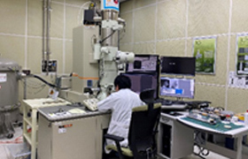 High Resolution Transmission Electron Microscope Lab
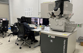 Focused lon Beam Lab
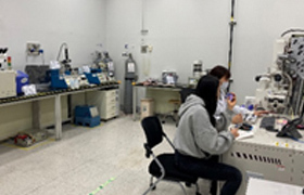 Scanning Electron Lab
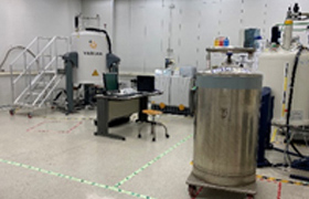 Nuclear Magnetic Resonance Spectroscope Lab
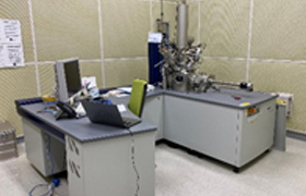 Secondary lon Mass Spectrometer Lab
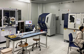 X-ray Analysis Lab
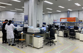 Integration Room 1
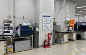 Integration Room 2
UEAC : UNIST Environmental Analysis Center
- It supports work of national certified certification institutions (persistent organic pollutants measuring institutions and education and research work for top-class environmental analysis.)
Environmental Analysis Center
| Contents | Details | ||
|---|---|---|---|
| Area | 422 ㎡ | Environmental Analysis Center New Nonorganic Analysis Lab |
|
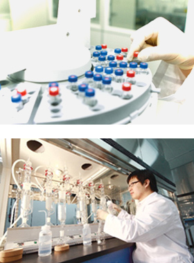
| Composition of Equipment | Organic analysis | 7 | GC/HRMS 3, LC/MS/MS, 2D GC/tof-MS, GC/MS, GC/ECD |
| Inorganic analysis | 4 | CP-TQ-MS, ICP-OES 2, LIBS | |
| Pretreatment | 34 | Rotary evaporator, Dry oven Heating mantle etc. | |
| Sampling device | 7 | Stack sampler 2, Gas analyzer 2, High volume air sampler 3 | |
| Total | 52 | Capable of analyzing micro-volume impurities | |
| Number of analysis / rate of operation | 1800 cases / 46.9% | It supported 1,800 cases of analysis with 46.9% rate of operation of equipment in 2020. | |
| Room class of the new Inorganic Analysis Lab | Under construction | Pre-processing room: 1000 class / Analysis Lab: 100 class | |
 GC/HRMS Lab
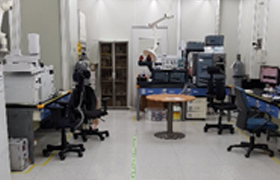 Organic Analysis Lab
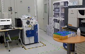 Inorganic Analysis Lab
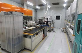 Pre-processing Room
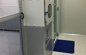 Pre-processing Room
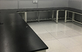 Inorganic Analysis Lab (100 class)
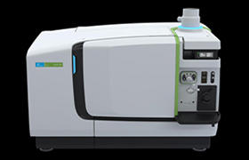 ICP-TQ-MS to be introduced(in 2021)
USRRL : UNIST Synchrotron Radiation Research Laboratory
- It supports diverse advanced researches leading basic sciences and development and researches of mext-generation energy materials, new drug materials, and next-generation display materials.
Conditions and Main Devices by Experiment Mode
| X-ray absorption sepecroscopy XAFS |
(Grazing) Small-angle X-ray scattering (GI) SAXS |
(Grazing) Small-angle X-ray diffraction (GI) WAXD |
X-ray single crystal Crystallography |
|
|---|---|---|---|---|
| Light source / spectroscope / resolution(ΔΕ/Ε) | Bending magnet / Si(111) dual crystal spectroscope / ~2×10⁻⁴ | |||
| Focusing mirror system | Toroidal, bendable (Coating materials: Rh 5 nm, Pt 35 nm) | |||
| Scope of Beam power(photen/s) / energy | 2×10¹¹ @10 keV / 520 keV | |||
| Beam size | (0.8 × 1.6) mm² | (0.6 × 0.8) mm² | (0.15 × 0.15) mm² | (0.12 × 0.12) mm² |
| Main experiment system |
|
|
|
|
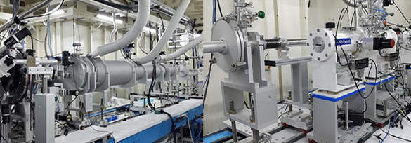
Composition of beam line
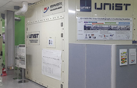 Entrance of 6D UNIST–PAL Beamline
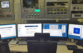 Data & EPICS PC
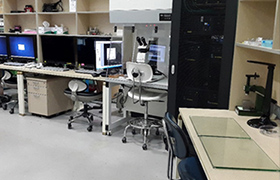 HKL2000 PC & Optical Microscopy
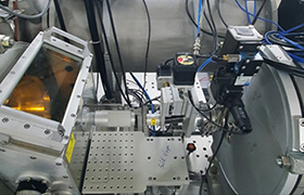
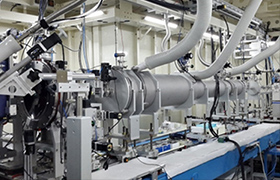 Experimental Hutch
Experimental mode
 (GI)-WAXD modes
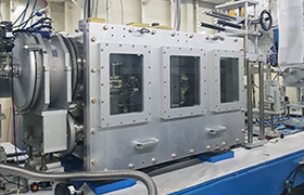 (GI)-SAXS modes
 X-ray crystallography mode
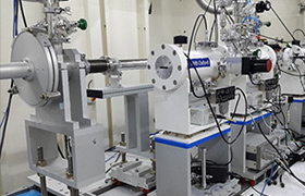 XAFS mode